AnsysGPT Coming Soon!!

Ansys, Inc. has taken the natural language processing engine to their products to create humanlike conversational dialog. This Ansys specific chatbot responds to questions and composes unique answers to various user inquires.  AnsysGPT is available in your native language and understands the underlying physics of the problems being queried so it can point you in the right direction.

What is AnsysGPT?

AnsysGPT is one of several products available in the Ansys AI family of software. It is a browser-based AI virtual assistant for all Ansys applications.  It is quite handy as it allows you to quickly seek answers and obtain links to source material with a simple query. AnsysGPT responds to you in a conversational tone with a solution to your question, often step-by-step, and reference material easily accessible that AnsysGPT used to derive its answer.


What Does AnsysGPT Cost and How Can I Access It?

AnsysGPT will be available and no cost to all Ansys customers with active commercial software subscriptions on July 1, 2024.   You will receive an email with instructions on how to activate AnsysGPT once your access has become available. For future software releases, AnsysGPT will have links embedded in the programs to quickly access the tool.

 Where Does AnsysGPT Get Its Information?

AnsysGPT draws from the Ansys created, developed, or licensed data that include, but is not limited to, Ansys Courses, articles, videos, webinars, product documentation, and other Ansys content.  AnsysGPT does not store any customer questions or input or derive any information from customer feedback. Users cannot add content to AnsysGPT to use as source material and all reference material is controlled by Ansys.

How Does AnsysGPT Work?

Users submit prompts to the chatbot that are related to Ansys products and services and AnsysGPT will respond and provide supporting documentation for its answers.   AnsysGPT is not a search tool, but generates new responses based on prompts submitted by the user.

If you would like to see AnsysGPT in action or interested in more information, please view our brief demonstration webinar.

Using Software to Meet EMC Standards for Electronics

Introduction 

Electromagnetic compatibility (EMC) is a critical aspect of electronic system design, especially for applications such as automotive, aerospace, defense, medical, and industrial. EMC ensures that electronic devices can operate without interfering with other devices or being affected by external electromagnetic fields. EMC also ensures that electronic devices comply with regulatory standards and customer expectations.

However, achieving EMC is not an easy task, as electronic systems become more complex, compact, and integrated. Designers and engineers need to consider various sources of electromagnetic interference (EMI), such as power supplies, cables, connectors, antennas, and printed circuit boards (PCBs). They also need to account for the effects of electromagnetic fields on the functionality, reliability, and safety of electronic components and systems.

One of the main sources of EMI in electronic systems is the PCB, which can act as a radiator or a receiver of electromagnetic fields. To reduce the EMI from the PCB, designers need to consider factors such as layout, routing, grounding, shielding, and filtering. Ansys EMC Plus allows you to simulate the electromagnetic behavior of your PCB, including the effects of cables, connectors, and enclosures.

To address these challenges, Ansys has developed a comprehensive solution for EMC analysis and verification: Ansys EMC Plus. Ansys EMC Plus is a powerful tool that enables you to simulate and optimize the electromagnetic performance of your electronic systems, from component to system level. With Ansys EMC Plus, you can:

  • Perform EMC pre-compliance testing and certification for various standards, such as CISPR, IEC, ISO, MIL-STD, and DO-160
  • Analyze and mitigate EMI issues, such as radiated and conducted emissions, susceptibility, and immunity
  • Optimize the EMC performance of your PCBs, cables, connectors, and enclosures
  • Validate the EMC performance of your electronic systems in realistic operating scenarios and environments
  • Integrate with Ansys Electronics Desktop and Ansys HFSS for seamless workflow and data exchange

In this blog post, we will introduce some of the key features and enhancements of Ansys EMC Plus 2024 R1, the latest release of Ansys EMC Plus. We will also show you how Ansys EMC Plus can help you design and verify electronic systems that meet EMC standards and performance requirements.

What’s New in Ansys EMC Plus 2024 R1?

GPU Accelerated Solver: A Game-Changer The new GPU Accelerated Solver is a standout feature, promising to revolutionize the way simulations are run. By harnessing the power of GPU acceleration, Ansys EMC Plus now executes simulations with unprecedented speed, making it a formidable tool in any engineer’s arsenal. Our webinar dives deeper into maximizing electronic performance.

The GPU Accelerated Solver is not only a game-changer for EMC simulations, but also for full PCB simulations. As shown in the image below, a full PCB simulation of a complex board only 3.2 hours on a GPU, compared to 53.5 hours on a CPU. This means that the GPU solver is 16.7 times faster than the CPU solver, enabling engineers to run simulations in a fraction of the time and iterate designs more quickly.

Visualization and Simulation: Seeing is Believing With the 3D Field and Current Visualization, engineers can now delve into the intricacies of electromagnetic fields with ease. The Transfer Impedance Simulator and the Radiation Pattern Probe further extend the software’s capabilities, offering detailed insights into complex electromagnetic phenomena.

Ansys EMC Plus delivers stunning 3D results visualization that lets you explore electromagnetic fields with unparalleled precision and clarity.

Enhanced Connectivity and Meshing: Precision Meets Efficiency The software’s ability to automatically assign cable wiring connectivity to 3D cables from mechanical CAD and its Direct Mesh Editing Features streamline the simulation process. The introduction of non-circular multiconductor transmission line conductor cross sections adds another layer of precision to the modeling.

Import and Integration: Bridging the Gap Ansys EMC Plus 2024 R1 boasts significant improvements in PCB Geometry Import, ensuring seamless integration and a smoother workflow. The Standalone Transient Circuit Solver and the integration with STK and EMC Plus Lightning Probability Tool exemplify the software’s commitment to comprehensive electromagnetic analysis.

Safety and Compliance: Ahead of the Curve Specific Absorption Rate (SAR) Modeling is a critical update, particularly for consumer electronics, where safety standards are stringent. This feature allows engineers to ensure compliance with international safety regulations, maintaining user safety as a paramount concern.

Conclusion: The Future of Electromagnetic Simulation Ansys EMC Plus 2024 R1 is a testament to the relentless pursuit of excellence in the field of electromagnetic simulation. With its robust features and user-centric enhancements, it stands as an indispensable tool for engineers looking to push the boundaries of electronics design.

How Can Ansys EMC Plus Help You?

Ansys EMC Plus can help you to design and verify electronic systems that meet EMC standards and performance requirements in various ways. Here are some examples:

  • Ansys EMC Plus can help you to perform EMC pre-compliance testing and certification for your electronic systems and avoid costly and time-consuming EMC failures and rework. You can use Ansys EMC Plus to simulate and verify the EMC performance of your electronic systems for various standards, such as CISPR, IEC, ISO, MIL-STD, and DO-160. You can also use Ansys EMC Plus to compare and optimize the EMC performance of different design alternatives and scenarios.
  • Ansys EMC Plus can help you to analyze and mitigate EMI issues for your electronic systems, and improve the functionality, reliability, and safety of your electronic systems. You can use Ansys EMC Plus to identify and locate the sources and paths of EMI, such as radiated and conducted emissions, susceptibility, and immunity. You can also use Ansys EMC Plus to evaluate and implement EMI mitigation strategies, such as shielding, filtering, grounding, and routing.
  • Ansys EMC Plus can help you to optimize the EMC performance of your PCBs, cables, connectors, and enclosures, and reduce the size, weight, and cost of your electronic systems. You can use Ansys EMC Plus to model and simulate the electromagnetic behavior of your PCBs, cables, connectors, and enclosures, and optimize their geometry, layout, and materials. You can also use Ansys EMC Plus to assess the impact of parasitics, losses, and dispersion on the EMC performance of your PCBs, cables, connectors, and enclosures.
  • Ansys EMC Plus can help you to validate the EMC performance of your electronic systems in realistic operating scenarios and environments and ensure the compatibility and interoperability of your electronic systems. You can use Ansys EMC Plus to simulate and verify the EMC performance of your electronic systems in various operating modes, such as idle, active, and standby. You can also use Ansys EMC Plus to simulate and verify the EMC performance of your electronic systems in various environments, such as near-field, far-field, and multipath.
  • Ansys EMC Plus can help you to integrate with Ansys Electronics Desktop and Ansys HFSS for seamless workflow and data exchange and leverage the power and versatility of Ansys electronics solutions. You can also use Ansys EMC Plus to perform field import with Ansys Electronics Desktop and Ansys HFSS, and achieve multi-scale EMC analysis and verification.

Conclusion

Ansys EMC Plus is a powerful solution for EMC analysis and verification, that enables you to design and verify electronic systems that meet EMC standards and performance requirements. Ansys EMC Plus 2024 R1 is the latest release of Ansys EMC Plus, that brings several new features and enhancements that improve the accuracy, efficiency, and usability of EMC analysis and verification. With Ansys EMC Plus, you can simulate and optimize the electromagnetic performance of your electronic systems, from component to system level, and across various domains, scales, and scenarios. Our experts offer a comprehensive webinar for designing and verifying electronic systems with unmatched EMC compliance.

The fastest time-to-value for complex device and platform EMI/EMC simulation.  

Ansys EMC Plus features a forgiving mesh and hybrid sub-cell solvers that allow for extreme geometric complexity without extreme user effort to clean and prepare geometry for simulation. Ansys EMC Plus also has a fast and intuitive user-interface that includes automated workflows and wizards to help inexperienced users become productive quickly. Ansys EMC Plus can import and merge 3D CAD geometry and cable database information automatically and create a consistent and complete model for EMI/EMC analysis. Ansys EMC Plus can also leverage the parallel computing power of GPUs to accelerate the simulation speed dramatically and provide more detailed results for larger models. 

Figure 4. EMC Plus Has a Short Time-to-Value by Making Analysis Fast and Easy to Learn 

EMC Plus is a useful addition to testing programs. Ansys EMC Plus can simulate various EMI/EMC tests, such as radiated emissions, radiated immunity, conducted emissions, conducted immunity, bulk current injection, transient immunity, etc. Ansys EMC Plus can also model the effects of different environments, such as ground planes, reverberation chamber, anechoic chamber, etc. Ansys EMC Plus can generate reports and plots that compare the simulation results with the standards and regulations and identify the sources and paths of EMI problems. Ansys EMC Plus can also perform parametric studies and design optimization to improve the EMI/EMC performance of the device or platform. 

EMC Plus provides seamless integrations with other Ansys tools and third-party software. Ansys EMC Plus can import and export data in various formats, such as STL, STEP, IGES, XLS, CSV, etc. Ansys EMC Plus can also interface with other Ansys tools, such Ansys HFSS, Ansys SIwave, or Ansys Material Intelligence, to perform multi-domain analysis of the device or platform. Ansys EMC Plus can also work Ansys optiSLang or with third-party software, such as MATLAB or Python, to perform custom scripting and automation of the simulation process. 

With these features and benefits, Ansys EMC Plus can help engineers in heavy industry to perform EMI/EMC analysis of their devices and platforms more efficiently and effectively, and to ensure compliance with the EMI/EMC standards and regulations. Ansys EMC Plus can also help engineers to reduce the cost and time of physical testing and prototyping, and to enhance the quality and reliability of their products. 

Ansys EMC Plus: A Tool for Heavy Industrial Applications 

Introduction 

Ansys EMC Plus is a tool for electromagnetic compatibility (EMC) and interference (EMI) analysis of heavy industrial vehicles and platforms. These vehicles must meet EMI/EMC requirements to ensure safety, reliability, and performance in harsh environments. Understanding whether a device will pass or fail an EMC test early in the product development cycle is essential to reducing cost and delays. However, most electromagnetic tools are not designed for full platforms and their cables, which can have complex geometries and interactions. Ansys EMC Plus, however, is designed for this purpose. It uses a hybrid approach that combines three solvers to solve the full platform model, including the 3D fields, the cables, and the nonlinear circuits. In this document, we will briefly introduce the tool and its features, and highlight some of the new capabilities in the 2024 R1 release that are relevant to heavy industry. 

Figure 1. Simulation of Radiated Emissions from a Full Vehicle Saves Cost and Risk  

Ansys EMC Plus Overview 

Ansys EMC Plus is a tool that enables engineers to perform EMI/EMC analysis of heavy industrial vehicles and platforms, such as trucks, buses, trains, ships, aircraft, and satellites. The tool can handle large and complex models with millions of mesh cells and thousands of cable segments and provides accurate and fast results. The tool can also simulate various EMC tests, such as radiated emissions, radiated immunity, conducted emissions, and conducted immunity, and help engineers identify and mitigate potential EMC problems. 

Ansys EMC Plus uses a hybrid approach that combines three solvers that operate simultaneously to solve the full platform model. The three solvers are: 

  • The 3D fields are solved with the finite difference time domain (FDTD) method. This method uses a grid-based mesh engine that is forgiving enough to be used with mechanical CAD geometry, without requiring extensive simplification or cleanup. The FDTD method can capture the complex interactions between the 3D fields and the platform, and account for the effects of shielding, apertures, and slots. 
  • The cables are solved with a modified multiconductor transmission line (MTL) theory solver that allows for all the cables on the platform, up to many thousands of segments, with a reasonable amount of analyst time. The MTL solver can model the effects of cable routing, twisting, bending, branching, and termination, and account for the coupling between the cables and the 3D fields. 
  • Finally, the ends of the cables may be solved with a transient nonlinear circuit (TNC) solver. The TNC solver can model the nonlinear behavior of electronic components, such as diodes, transistors, and integrated circuits, and account for the effects of voltage and current sources, loads, and switches. 

The hybrid approach of Ansys EMC Plus enables engineers to perform EMI/EMC analysis of full platforms and their cables with high accuracy and efficiency, and to evaluate the performance of the devices under various EMC scenarios. 

New Features in 2024 R1 Release 

Ansys EMC Plus has new features in its 2024 R1 release that are relevant to heavy industry. These features include a new capability to automatically merge the 3D CAD geometry and the cable database information. Most manufacturers track the path of cables in 3D CAD, while the wiring diagram is stored in cable database software. Ansys EMC Plus can now automatically import and merge these disparate sources of data and create a consistent and complete model for EMI/EMC analysis. This feature can save time and reduce errors in the model creation process. 

Figure 2. New Feature Allows Merging 3D Cable Paths from CAD with Wiring Assignments from Cable Database Software  

A new GPU solver that increases the simulation speed dramatically. The GPU solver can leverage the parallel computing power of graphics processing units (GPUs) to accelerate the FDTD method. The GPU solver is about 12 times faster than the previous CPU version, making the tool even easier to use for complex geometry. The GPU solver can also handle larger models with more mesh cells and provide more detailed results.  

Figure 3. EMC Plus GPU Solver is Almost 12 Times Faster than the Previous CPU Version 

These new features of Ansys EMC Plus can help engineers in heavy industry to perform EMI/EMC analysis of their vehicles and platforms more efficiently and effectively, and to ensure compliance with the EMC standards and regulations. 

The fastest time-to-value for complex device and platform EMI/EMC simulation.  

Ansys EMC Plus features a forgiving mesh and hybrid sub-cell solvers that allow for extreme geometric complexity without extreme user effort to clean and prepare geometry for simulation. Ansys EMC Plus also has a fast and intuitive user-interface that includes automated workflows and wizards to help inexperienced users become productive quickly. Ansys EMC Plus can import and merge 3D CAD geometry and cable database information automatically and create a consistent and complete model for EMI/EMC analysis. Ansys EMC Plus can also leverage the parallel computing power of GPUs to accelerate the simulation speed dramatically and provide more detailed results for larger models. 

Figure 4. EMC Plus Has a Short Time-to-Value by Making Analysis Fast and Easy to Learn 

EMC Plus is a useful addition to testing programs. Ansys EMC Plus can simulate various EMI/EMC tests, such as radiated emissions, radiated immunity, conducted emissions, conducted immunity, bulk current injection, transient immunity, etc. Ansys EMC Plus can also model the effects of different environments, such as ground planes, reverberation chamber, anechoic chamber, etc. Ansys EMC Plus can generate reports and plots that compare the simulation results with the standards and regulations and identify the sources and paths of EMI problems. Ansys EMC Plus can also perform parametric studies and design optimization to improve the EMI/EMC performance of the device or platform. 

EMC Plus provides seamless integrations with other Ansys tools and third-party software. Ansys EMC Plus can import and export data in various formats, such as STL, STEP, IGES, XLS, CSV, etc. Ansys EMC Plus can also interface with other Ansys tools, such Ansys HFSS, Ansys SIwave, or Ansys Material Intelligence, to perform multi-domain analysis of the device or platform. Ansys EMC Plus can also work Ansys optiSLang or with third-party software, such as MATLAB or Python, to perform custom scripting and automation of the simulation process. 

With these features and benefits, Ansys EMC Plus can help engineers in heavy industry to perform EMI/EMC analysis of their devices and platforms more efficiently and effectively, and to ensure compliance with the EMI/EMC standards and regulations. Ansys EMC Plus can also help engineers to reduce the cost and time of physical testing and prototyping, and to enhance the quality and reliability of their products. 

Importance of Thermal Analysis in PCB Life Prediction

Electronic devices are built on a printed circuit board (PCB), which serves as the foundation that provides the power supply and allows communication between the different devices. Reliability of the PCB is critical to ensure that these electronic devices remain connected, avoiding malfunctions and ensuring the device performs its intended functions for extended periods of time. There are a variety of failure modes that can affect the reliability of a PCB that are discussed in a webinar that DRD Technology conducted, but the subject of this paper is specific to failure due to thermal cycling.

During operation a PCB can undergo a process known as thermal cycling, which is referred to as the repeated exposure of a PCB to fluctuations in temperature during its operational lifecycle. The fluctuations in temperature can be caused by normal operation of the PCB or changes in the environment it is exposed to. These variations in temperature over time can have a profound impact on the solder joints and significantly reduce the life span of the PCB.

As a PCB heats up and cools down through a process known as thermal cycling, there is a phenomenon known as thermal expansion mismatch due to the different materials that make up the board and its components. This cyclic loading causes mechanical strain that may eventually cause the solder joints to gradually deteriorate by causing fractures, cracks, and ultimately failure. These failures or malfunctions may result in erratic electrical connections, degenerate signal quality, or total device malfunctions, all of which can have serious repercussions by reducing the lifespan of the product.

There is a tool within the Ansys portfolio of products called Sherlock that provides fast and accurate life predictions for a PCB early in the design process. Sherlock enables engineers to break free from the design-build-break-repeat cycle that is common in the industry by empowering designers to quickly evaluate the probability of failure due to mechanical, and yes, thermal stress. Sherlock can also be used as a preprocessor for thermal analysis by identifying board level components and assigning material properties appropriately, which can save the designer a significant amount of time.

ECAD Preprocessing in Sherlock

Ansys Sherlock can read all major ECAD formats and can be used as a preprocessor for FEA and CFD analysis to save a significant amount of time. There is an extensive library of parts (over 600,000) and materials within Sherlock that can be used to automatically create geometry and assign material properties, which can reduce preprocessing times an order of magnitude – days to minutes. Sherlock will track over all the details in the ECAD and automatically extract part information from the CAD files, parts list, BOM, etc. See below parts list in Sherlock after reading in ECAD:

Sherlock references a collection of internal databases when assigning material and properties to board components. This streamlined feature can save the analyst a significant amount of time, but it is important to review the part properties and correct them as needed to ensure accurate results. Once the material and properties have been checked for accuracy, the project can be exported into the Ansys Electronics Desktop (AEDT) environment for thermal analysis.

Thermal Analysis in Icepak

It is important to provide Sherlock with accurate board and component level temperatures when predicting the board service life. Without simulation, the analyst would need to rely on experimental data which can be time consuming to produce because it requires a PCB to be manufactured and an experimental procedure developed to mimic conditions in the field. Incorporating thermal analysis early in the design process can provide accurate temperatures for life predictions without which can accelerate product development and reduce costly mistakes that require redesign.

An analyst can read in the exported project from Sherlock and all the materials and associated properties will automatically be assigned. A board can have a great number of components, so using Sherlock as a preprocessor can save the analyst a significant amount of time. See below temperature and velocity field from a thermal analysis solved in Icepak for a board experiencing forced convection cooling:

The temperature values on the board from the thermal analysis can be exported into a temperature map file that can be read into Sherlock for accurate thermal cycling. Accurate temperatures are important when predicting the probability of failure due to thermal cycling in solder fatigue analysis.

PCB Life Prediction in Sherlock

Bringing in accurate temperature values and distribution into Sherlock is critical when making life predictions. Sherlock can import images from heat maps found experimentally or temperature map files from thermal simulations. The benefit of using a temperature map file from thermal analysis is that the board does not even need to be manufactured. The analyst simply needs to read the results from Icepak into Sherlock to map the temperatures onto the board for accurate thermal cycling analysis. See below an image of the results from the thermal analysis in the previous section getting mapped onto the board in Sherlock:

If the thermal cycle of the board is such that it simply powers on and off, then only a single temperature map from Icepak may be required if you can assume the off-power state reaches ambient conditions – the analyst only needs a temperature map file that represents the on-power state. There are various scenarios that would require multiple temperature map files to be read into Sherlock for thermal cycling analysis. For example, if the board has high and low-power states, the analyst will want to create a temperature map file for each state of the board to read into Sherlock for thermal cycling. The user can easily specify a maximum and minimum temperature state for the thermal cycle to account for the low and high-power state of the board, as well as ramp and dwell times.

Once the maximum and minimum temperature of the thermal cycle has been defined, a sold fatigue study can be conducted to predict the life of the board. See below:

Reviewing the life prediction graph above indicates that there is a 45 percent change of failure due to thermal cycling. Catching issues like this early in the design process is critical in bringing products to market on time and budget.

Conclusion

Thermal cycling poses a significant risk to the reliability of solder joints in PCB design. The use of virtual prototyping early in the design process allows for a good understanding of the temperature load the PCB will be subjected to in the field, which leads to accurate solder fatigue analysis before the need to manufacture the board and gather experimental data. Integrating simulation into the design process enables engineers to ensure the long-term performance and reliability of electrical devices by identifying thermal issues early. Identifying and resolving the effect of temperature cycling on solder fatigue is essential to producing products that meet or surpass today’s needs in a world where electronics reliability is non-negotiable.

Thermal Management Solutions for Electronics

Thermal management of electronics is essential to a product’s dependability, efficiency, and lifespan.  Incorporating thermal analysis early in the design process is not just best practice, but necessary for engineers to deliver high-quality products in the ever-changing landscape of electronics design. Modern electronics are increasingly more complex and compact, and using engineering simulation allows engineers to test their design under real-word conditions in a virtual space to reduce physical testing and redesign.

Overheating can lead to performance degradation, accelerated aging, or catastrophic failures. Identifying excessive heat buildup early in the design process can reduce costs and accelerate product development by helping engineers identify hot spots so they can implement effective cooling strategies. Through thermal analysis, engineers can also understand the thermal interaction between components in an electronics enclosure and adjust the spatial arrangement to ensure long-term reliability and mitigate design risks which will streamline the design process.

Electro-Thermal Analysis of PCB

The modern PCB often contains complex circuitry with numerous components that must fit into a small space. The PCB design process must accommodate for this complexity while balancing the signal integrity, power distribution, thermal management, and manufacturability of the design. Ansys has several electronics and thermal simulation tools that are often used in concert to make informed decisions and mitigate risk for PCB design. DRD Technology has also published a webinar on some of these workflows on their website.

In Ansys Electronics Desktop (AEDT), a DCIR analysis is a valuable tool for PCB design that enables informed decision making around the application requirements. It is often used to understand voltage drops that can affect the performance of active components, identify regions of high current density that can cause hot spots, optimize the placement and thickness of traces, and other design issues. Detecting these early in the design process saves time and money associated with physical prototyping and testing. The losses measured in the DCIR analysis can be mapped onto the board for thermal analysis. These board losses can have a significant impact on the temperature field in electronics devices. In the simple electronic system below, the thermal model on the left does not have losses from the board incorporated, whereas the thermal model on the right does:

In the example above, incorporating the board losses into the thermal model provides a more accurate representation of the temperature field so an engineer can make informed decisions around cooling strategies. There is a rule of thumb often used when designing electronics with electrolytic capacitors, and that is for every increase in 10 degrees centigrade, the life of the capacitor is cut in half. This can make it crucial to include board losses in your thermal solution to provide detailed insight into how long the design will last.

Electro-Thermal Analysis of Waveguide Filter

For both military and commercial applications, waveguide filters are essential to modern radar and satellite communications. Waveguide filters with the ability to operate in a variety of challenging conditions and high-power loads are in greater demand. To better understand heat generation, distribution, and dissipation inside the waveguide structure, thermal simulation must be incorporated early in the design process.

By simulating the thermal conditions a wave guide filter will be subjected in a virtual environment, engineers can identify thermal related issues early in the design phase, implement effective cooling strategies and ensure appropriate materials are incorporated. Excessive heat buildup can cause mechanical deformation due to thermal stresses that can affect the filter’s performance and cause material degradation. Through virtual prototyping, the thermal characteristics of the wave guide filter under real world conditions can be simulated, and engineers can maintain acceptable temperature ranges which will ensure long term performance of the filter.  

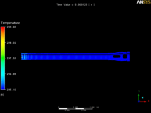
The electromagnetic and thermal performance of a wave guide filter can be evaluated within AEDT. Once an engineer has evaluated the electromagnetic performance of their design, the electrical losses can be converted into a thermal solution under real-word conditions. Below is an image of a thermal model that represents the waveguide filter subjected to force convection cooling to get an understanding of the temperature distribution.

This temperature field can then be converted into thermal stress and to get an idea of how the structural will deform in the field. Studying the thermal effects of the waveguide helps engineers identify areas of high thermal stress and design the filter that ensures long-term durability and reliability.

Electro-Thermal Analysis of Electric Motor

Electric motors are found throughout modern society, powering everything from household appliances to industrial machinery. They are responsible for 38.4% of the U.S. electrical energy consumption based on published information from the U.S. Department of Energy, which drives demand for new energy efficient designs. Managing the thermal aspects of these new energy efficient electric motors is often one of the most challenging aspects of the design process, and incorporating simulation early in the design process will help ensure these motors meet the high-performance requirements of modern applications.

What makes thermal management essential in electric motor design is the impact temperature can have on reliability and performance. Excessive heat can build up and degrade insulation, cause premature bearing wear, and cause demagnetization, all of which will reduce the efficiency and lifespan of the electric motor.  Thermal analysis will enable engineers to explore various cooling techniques and configurations in a virtual environment to quickly improve thermal management systems and bring products to market faster.

Ansys has electrical and thermal solutions for electrical motors. An engineer can evaluate the performance of their design withing AEDT, and once the performance of the electric motor has been evaluated and deemed appropriate for the application, the losses can be converted into a thermal solution. The stator of an electric motor is often where most of the heat is generated, and these losses can accurately be accounted for. In the image below the losses in the stator are mapped over into a tool called Ansys Fluent.

Conclusion

Thermal analysis is a fundamental component of electronics design that enables engineers to maximize efficiency, reliability, and performance by providing insight into the thermal behavior of the electrical system. By incorporating thermal analysis early in the design process, engineers can proactively handle thermal challenges, reduce design risk, and produce reliable, high-quality devices that satisfy changing market demands. In today’s competitive landscape, adopting thermal analysis as a core component of the design process is not only advantageous, but necessary for success.

Using Ansys Mechanical Software to Model Cracks (Part 3 of 3 in a series on Fracture Mechanics)

In our last blog post of this series, I dive into how we can simulate cracked structures using Ansys simulation software, Ansys Mechanical. As before, if you’ve not read the previous two posts, go back and read ‘em!!! 

How Engineers Use Ansys Mechanical Software to Model Cracks 

Ansys Computer Aided Engineering (CAE) simulation software allows engineers to study cracks in structures via fracture mechanics, along with a host of other structural simulation needs. Ansys has a long history of simulation development since the 1970’s in creating tools for engineers to design and virtual prototype their products. As a quick note, Ansys is not limited to just structural physics either. Fluids, electromagnetics, systems and optics are some of the other fields Ansys offers in its portfolio of simulation capabilities. 

The options to create a crack in Ansys simulation software generally fall in two categories: either a) use a CAD surface that represents the crack, that overlaps with the structure or b) use the auto-generation tool in Ansys to add a crack at the mesh level. 

The former works well in all scenarios but is very useful when the crack is not a simple analytical shape, i.e., a penny-shaped crack. The latter is great for those simple, penny-shaped cracks, where the engineer can input two radii to define the shape, input where the crack is located, and they’re done. 

Here’s an example; take this simplified cast bearing/shaft support. The machinist finds a crack when machining the bearing support housing (outlined in the blue box). Perhaps this is caused by an incorrect casting process. 

Representative CAD Model, Crack Surface on Right 

When magnafluxed or cut open, the crack is not a simple shape. This is perhaps an extreme example, but it gets the point across. With a few inputs and clicks, Ansys overlaps the crack surface with the solid CAD, splits the mesh where these intersect, buffers the elements from the new crack mesh into the existing base mesh, and voila! The finite element model crack is ready to analyze.

Representative Finite Element Mesh of Structure with Crack Inserted: Back View on Left, Top View on Right (with red line indicating part boundary) 

What About Crack Growth? 

Ansys requires no special treatment of the crack to determine the relevant fracture parameters when evaluating a crack for simple comparison to material fracture toughness. The simplicity of the Ansys workflow mirrors the simplicity of what the engineer is after, i.e., a single value for Stress Intensity Factor. Using the methods described previously, engineers can model a crack and then mesh the structure with hexahedra, tetrahedra, or a mix of element shapes and get results for Stress Intensity Factor. 

For fatigue cracks, the requirements are greater. Engineers must provide the crack growth equation constants, i.e., the Paris constants C and m, then Ansys will do the rest. Ansys’ technology for general, 3D crack growth is quite extraordinary. This technology is referred to as SMARTSeparating, Morphing, and Adaptive Remeshing Technology. To put it simply, automatic remeshing occurs as the crack grows in simulation. 

Representative Crack Growth Simulation Showcasing Automated Solution Remeshing 

For a nice overview of fracture mechanics in Ansys, you can watch an on-demand webinar on DRD’s website. In the webinar, I provide a brief overview of fracture mechanics and Ansys capabilities in fracture analysis, much like this paper. I also discuss damage tolerant design, material data acquisition, and Ansys CAE simulation of cracks in structures. 

Head over to DRD’s website for two on-demand webinars I conducted in October and November, ‘Simulating Crack Propagation Part 1 and 2.’ 

https://www.drd.com/resources-all/simulating-crack-propagation-part-1-webinar-recording/ 

https://www.drd.com/resources-all/simulating-crack-propagation-part-2-webinar-recording/ 

This concludes our 3-part series on fracture mechanics. We have a few other resources engineers can dig into on this topic, including the two on-demand webinars mentioned above. DRD has a fracture mechanics training course that I teach as demand requires, https://www.drd.com/project/ansys-mechanical-fracture-mechanics/. If you are interested in this course, please let us know at support@drd.com.